Monday, November 05, 2012

WEEK 14: 5TH NOVEMBER 2012


Title            : Preparing for Engineer’s Day on 8th November                                2012.

Objectives  : 1) To make sure the poster had been done.
                      2) To make a preparation for the presentation.
                      3) To make sure the project is function well to                                     demonstrate to the assessors.

Procedures: 1) During the Engineer’s Day, the student must do a                           demonstration and presentation of the project at                             Gemilang Hall.

                     2) The draft of the poster had been shown to the                                 supervisor and been printed in A1 size.

Results:

Figure 1: The Smart Chicken Coop poster for the project presentation and demonstration during Engineer's Day. 


Conclusion: The project presentation and demonstration are successfully done and going smoothly. The assessors and the lecturer that attract with the Smart Chicken Coop were giving a lot of knowledge and suggestion to improve in future to make it more marketable. The draft of the report and logbook will be submitted in Week 14 and the hard covered final report will be submitted in Week 17.

Thursday, October 25, 2012

WEEK 13: 25TH OCTOBER 2012


Title             : Testing and demonstrating all the components and                         circuits of the Smart Chicken Coop.

Objective    : To make sure all the component and circuit are                               function well as been plan according to the                                       flowchart.

Procedures : 1) The thermistor and humidity sensor operation                                  had been shown in Video 1.

                       2) The water level sensor operation had been                                      shown in Video 2.

Results:
Video 1: Testing the bulb and fan

1) For the bulb, when the temperature in the chicken coop was 30°C and below, the bulb will turned ‘on’ to produce heat in the chicken coop. The bulb will remain turned ‘on’ until the temperature inside the chicken coop was 30°C and above, then it will turn ‘off’. It will remain turned ‘off’ until the temperature was 30°C.

2) For the fan, when the humidity in the chicken coop was 59% and below, the fan was turned ‘off’. The fan will remain turned ‘off’ until the humidity was 60% and above, then it will turned ‘on’ to give an air circulation in the chicken coop because the humidity was high.

Video 2: Testing the water pump

3) The water pump was turned ‘on’ and remaining refill the water in the container inside the chicken coop when the water was getting empty. At this time, the water level sensor will detect the water in the container inside the chicken coop was in a low level. It will stop refilled the water from main supply water outside the chicken coop when the water level sensor detect the water was getting full. At this time the water pump was turned ‘off' automatically. 

Conclusion: Overall, this project was successfully function according to the flowchart. The current problem encountered was the bulb was blinking sometimes. This is because temperature is always changing and unexpected. It was blinking when there was an interchanging between 30°C and 31°C. The adapter that been used in this project are also not enough supply current because when the water pump was turned ‘on’ the bulb and LCD was blinking and unstable. This problem can be overcome in future by changing the adapter that has high current than the existing that been used in this project.

WEEK 12: 25TH OCTOBER 2012


Title              : Attach the circuit and component with hardware,                              burned the program into IC’s and test the water                              level sensor.

Objective     : To make sure the hardware is suitable with the                                function of the project.

Procedures : 1) The IR distance sensor circuit, humidity sensor                              circuit, thermistor circuit, water level sensor                                      circuit had been attach on the top space inside                                the chicken coop.

Figure 1: All the circuits had been attached on top space inside the chicken coop

Results     : 1) The components had been attached with the                                   hardware: 

Figure 2: The thermistor had been hanging on top inside the chicken coop

Figure 3: The bulb had been attached on top inside the chicken coop

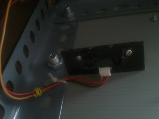
Figure 4: The IR distance sensor had been attached on the right side inside the chicken coop by facing it downwards.

Figure 5: The fan had been attached on the right side outside the chicken coop

Figure 6: The water level sensor had been attached with the water container inside the chicken coop

Figure 7: The water pump had been attached on top of the water container inside the chicken coop

Figure 8: The humidity sensor had been attached on the left side inside the chicken coop


             2) The water level sensor had been tested. The results                       had been made in illustration below: 

Figure 9: Illustration of water level sensor


Conclusion: All the circuit and component had successfully                                attached with the hardware and suitable with its                                function and the program had been burned into the                        IC and ready to be tested.

Wednesday, October 17, 2012

WEEK 11: 17TH OCTOBER 2012


Title            : Designing the hardware of Smart Chicken Coop.

Objective   : To design a simple, practicable, and convenience                          hardware to the user.

Procedure  : 1) The hardware had been design using Google                                 SketchUp software. 

Figure 1: Front view

Figure 2: Side view

Figure 3: Back view

Figure 4: Top view

                  2) The material that been use to design the real                                    hardware are steel, screw, nuts, cardboard,                                      prospect and fence. 

Figure 5: Steel

Figure 7: Screw and nuts

Figure 8: Cardboard

Figure 9: Prospect

Figure 9: Fence

                 3) Those material had been screwed to make the                                Smart Chicken Coop hardware according to the                              design that been sketch.

Figure 10: The steel had been screwed to build the base frame

Figure 11: The cardboard had been attached to the base frame


Result: 

Figure 12: The hardware of Smart Chicken Coop           


Conclusion : The hardware part can be imagine by sketching the                         hardware design using Google SketchUp. The full                           image can be imagine because it is a 3D software.

Friday, October 12, 2012

WEEK 10: 12TH OCTOBER 2012


Title           : Testing the LCD, bulb, and thermistor sensor                                 circuits.

Objective   : To make sure the circuits are function well.

Procedure : 1) The LCD circuit had been tested. When the                                    toggle switch (as shown in Figure 1) been ‘on’, the                          system will start operate by displaying ‘SMART                              CHICKEN COOP LOADING!!!’ (as shown in                                    Figure 2) followed by the surrounding                                              temperature, the percentage of humidity, and the                            condition of fan, bulb, and feeder motor (as shown                          in Figure 3) at the 20x4 LCD.

                                   Figure 1: Toggle switch

 Figure 2: The system will start operate by displaying ‘SMART CHICKEN COOP LOADING!!!’

Figure 3: The surrounding temperature, the percentage of humidity, and the condition of fan, bulb, and feeder motor

                2) Next thermistor sensor had been tested. When the                         surrounding area is in room temperature, the bulb will                     turned ‘on’.

              Figure 4: Thermistor sensor in room temperature

                                 Figure 5: The bulb turn ‘on’

                  3) The thermistor had been burn by using the lighter.

                   Figure 6: Thermistor sensor is above 30°C

                                Figure 7: The bulb turn ‘off’


Results: 


Conclusion: The LCD, bulb, and thermistor sensor circuits are                            function well.

Friday, October 05, 2012

WEEK 9: 5TH OCTOBER 2012


Title             : Write the programming by using Arduino Alpha                               software.

Objectives   : To write the program accordingly and similar with                            the function of the project.

Procedure   : 1) The Arduino Alpha software had been installed.

                            Figure 1: Arduino Alpha software

                    2) The new window to write the program had been                             displayed.

           Figure 2: The new window of Arduino Alpha software

Result         : The program for Smart Chicken Coop had been                             written according to the function.


               Figure 3: The program for Smart Chicken Coop

Conclusion: The program will be burn into Atmega 328 by using                        the IC burner.

Friday, September 28, 2012

WEEK 8: 28th SEPTEMBER 2012


Title             : Designing the PCB (Printed Circuit Board).

Objective    : To design the PCB layout by printing the PCB                                 circuit, etching, drilling, placed the components,                             soldering the components and testing the circuits.  

Procedures: 1)   The design of a Printed Circuit Board (PCB)                                   layout of the system was printed on the                                             Overhead Projector (OHP) plastic.                                
                        Figure 1: PCB layout printed on OHP paper

                       2)   The masking tape had been used to stick the                                  printed OHP plastic with copper board and make                            sure there was no air bubble between both. This is                          the important step so that the circuit had been                                  transfer perfectly onto the PCB board without any                            broken connection.

   Figure 2: Masking tape had been stick with copper board

            3)   Then, a paper or cloth had been covered on the                     board to avoid the plastic melts due to the                             transparency of its hot iron. The iron had been set to             ‘Linen' or as high as the iron will go. A fairly hot iron               was needed because the toner had been forced to               melt and subsequently bond to the copper blank                   PCB.

Figure 3: Ironing the covered board

   4)   Then, the ironed circuit had been leaved for a while      to cool it down. Do not remove the masking tape          when the board still hot. After it cool, the masking        tape had been removed. The circuit that been iron      had been shown below.

Figure 4: The circuit after been ironed

    5)   Next the connection of the circuit had been check       by using the multimeter. The multimeter had been       set to ‘beep’ sound. The multimeter will produce a       ‘beep’ sound when the connection is connected to       each other. If no ‘beep’ sound was produce, the           connection might be broken.

Figure 5: The connection had been check using multimeter

   6)   The defects connection had been touch up by using    permanent marker pen 700 artline.

Figure 6: 700 artline permanent marker had been use to touch up the defects connection


  7)   Next, the etching process had been proceed by pouring some hydrochloric acid on a plastic container and soak in the copper board into the acid. The container then had been shaking slowly to remove the copper layout from the board.  

Figure 7: The copper board had been soak into the Hydrochloric acid 

           8)   Then the circuit board had been washed using clean            running water and been brushed with very fine grade            of sand paper. This will remove dirt, oils and other                contamination on the top of the PCB board. After                  rinse, the board had been dried quickly by wiping it                with towels wet with acetone. The wiping step had                been repeated as many times needed until the                      paper towel comes off completely clean. The board              had been dried quickly to avoid oxidization.

                         Figure 8:The circuit after etching

           9)   Next the etching circuits had been clean by rubbing              the circuit with very fine sand paper to remove the                copper layer. 

 Figure 9: The etching circuits had been clean with very fine sand paper

           10)   Then the circuit had been drill to make a hole for                    electronic component placement.

Figure 10: The circuit had been drill by using hand drill

Figure 11: The PCB board after being drilled

            11)   Next, the component had been placed by referring               the schematic diagram and been soldered.

Figure 12: The component had been soldered

 12)   After that, the component leg had been cut off by using a cutter. 

Figure 13: The soldered component's leg had been cut

 13) The connection of the circuit had been check again      by using multimeter. The multimeter had been set to    ‘beep’ sound. The multimeter will produce a ‘beep’      sound when the connection is connected to each        other. 

Figure 14: The connection had been check using multimeter

14)   If no ‘beep’ sound was produce, the connection           might be broken. The connection can be overcome     by soldering a little jumper wire on downside of the     PCB board to make it connected.

Figure 15: The jumper wire had been soldered to the defected circuit connection

Figure 16: The final PCB board after being through the above step 

Conclusion: Basically, the PCB process consisting six                               processes which are printing the PCB circuit,                         etching, drilling, placed the components,                                 soldering the components and testing the circuits.